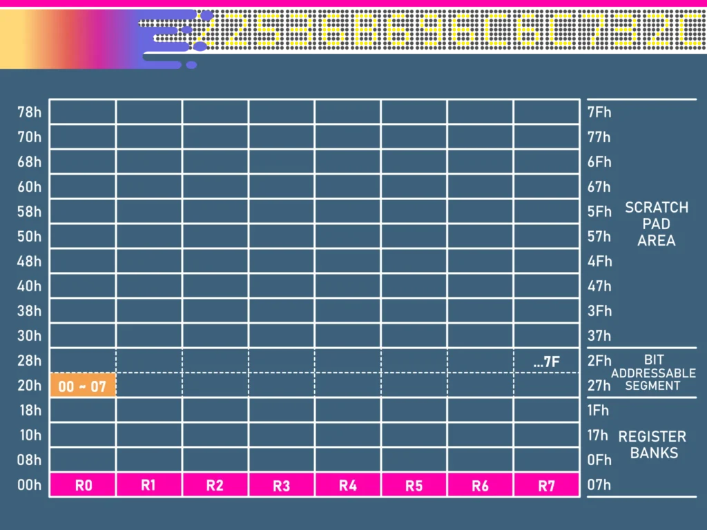

The 128 Bytes of RAM which can be accessed by both direct and indirect addressing can be divided into 3 segments as shown in picture.
- Register Bank 0~3 : Location 0 through 1Fh (32 bytes). ASM-51 and the device after reset default to register bank 0. To use the other register banks the user must select them in the software. Each register bank contains 8 one-byte registers, 0 through 7. Reset initiallizes the Stack Pointer to location 07h and it is incremented once to start from location 08h which is the first register (R0) of the second register bank. Thus, in order to use more than one register bank, the SP should be initialized to a difference location of the RAM where it is not used for data storage (ie, higher part of the RAM).
- Bit Addressable Area : 16 bytes have been assigned for this segment, 20h-2Fh. Each one of the 128 bits of this segment can be directly addressed (0-7Fh). This bits can be referred to in two ways both of which are acceptable by the ASM-51. One way is to refer to their addresses, ie, 0 to 7Fh. The other way is with reference to bytes 20h to 2Fh. Thus, bits 0-7 can also be referred to as bit 20.0-20.7, and bits 8-Fh are the same as 21.0-21.7 and so on. Each of the 16 bytes in this segment can also be address as a byte.
- Scratch Pad Area : Bytes 30h through 7Fh are available to user as data RAM. However, if the stack pointer has been initialized to this area, enough number of bytes should be left aside to prevent SP data destruction.
Post Views: 8